Working Principle of Solar Panels? Solar PV?
Of the Developing Renewable Energy sources,
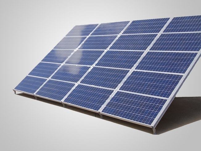
The most famous one is a Solar PV panel,
Also referred to as Solar Plate.
What is a Solar PV cell and How Does it Work?
It involves Some Neat Physics, Chemistry, and Mathematical Trick.
Let’s Learn how !
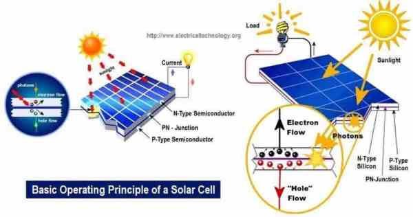
The conversion of light energy in electrical energy is based on a phenomenon called the photovoltaic effect.
Thus the name – Solar PV –
PV means Photo Voltaics!
When semiconductor materials are exposed to light, the some of the photons of light ray are absorbed by the semiconductor crystal which causes significant number of free electrons in the crystal.
This is the basic reason of producing electricity due to photovoltaic effect.
Photovoltaic cell is the basic unit of the system where photovoltaic effect is utilized to produce electricity from light energy. Silicon is the most widely used semiconductor material for constructing photovoltaic cell.
The silicon atom has four valence electrons. In a solid crystal, each silicon atom shares each of its four valence electrons with another nearest silicon atom hence creating covalent bond between them.
In this way, silicon crystal gets a tetrahedral lattice structure. While light ray strikes on any materials some portion of the light is reflected, some portion is transmitted through the materials, and rest is absorbed by the materials.
The same thing happens when light falls on a silicon crystal. If the intensity of incident light is high enough, sufficient numbers of photons are absorbed by the crystal and these photons, in turn, excite some of the electrons of covalent bonds.
These excited electrons then get sufficient energy to migrate from the valence band to the conduction band. As the energy level of these electrons is in conduction band they leave from the covalent bond leaving a hole in the bond behind each removed electron.
Too much to understand ,
Read Further,
These are called free electrons move randomly inside the crystal structure of the silicon. These free electrons and holes have a vital role in creating electricity in photovoltaic cells.
These electrons and holes are hence called light-generated electrons and holes respectively.
These light-generated electrons and holes cannot produce electricity in the silicon crystal alone. There should be some additional mechanism to do that.
When a pentavalent impurity such as phosphorus is added to silicon the four valence electrons of each pentavalent phosphorous atom are shared through a covalent bond with four neighbor silicon atoms and fifth valence electron does not get any chance to create a covalent bond.
This fifth electron then relatively loosely bounded with its parent atom.
Even at room temperature, the thermal energy available in the crystal is large enough to disassociate these relatively loose fifth electrons from their parent phosphorus atom. While this fifth relatively loose electron is disassociated from parent phosphorus atom, the phosphorous atom immobile positive ions.
The said disassociated electron becomes free but does not have any incomplete covalent bond or hole in the crystal to be re-associated. These free electrons come from pentavalent impurity are always ready to conduct current in a semiconductor.
Although, there are numbers of free electrons but still the substance is electrically neutral as the number of positive phosphorous ions locked inside the crystal structure is exactly equal to the number of the free electrons come out from them.
The process of inserting impurities in the semiconductor is known as doping and the impurities are doped are known as dopants. The pentavalent dopants which donate their fifth free electron to the semiconductor crystal are known as donor. The semiconductors doped by donor impurities are known as n-type or negative type semiconductor as there are plenty of free electrons which are negatively charged by nature.
When instead pentavalent phosphorous atoms, trivalent impurity atoms like boron are added to a semiconductor crystal totally opposite type of semiconductor will be created.
In this case, some silicon atoms in the crystal lattice will be replaced by boron atoms in other words the boron atoms will occupy the positions of replaced silicon atoms in a lattice structure. Three valance electrons of boron atom will pair with valance electron of three neighbor silicon atoms to create three complete covalent bonds.
For this configuration, there will be a silicon atom for each boron atom, fourth valance electron of which will not find any neighbor valance electrons to complete its fourth covalent bond.
Hence this fourth valance electron of these silicon atoms remains unpaired and behaves as incomplete bond. So there will be a lack of one electron in the incomplete bond and hence an incomplete bond always attracts electron to fulfill this lack. As such, there is a vacancy for electron to sit.
This vacancy is conceptually called positive hole.
Check this Video out
In a trivalent impurity-doped semiconductor a significant number of covalent bonds are continually broken to complete other incomplete covalent bonds.
When one bond is broken one hole is created in it.
When one bond in completed, the hole in it disappears.
In this way one hole appears to disappear another neighbor hole. As such holes are having relative motion inside the semiconductor crystal.
In the view of that it can said that holes also can move freely as free electrons inside semiconductor crystal.
As each of the holes can accept electron, the trivalent impurities are known as acceptor dopants and the semiconductors doped with acceptor dopants are known as p-type or positive type semiconductors.
In n-type semiconductors mainly the free electrons carry a negative charge and in p-type semiconductors mainly the holes, in turn, carry positive charge therefore free electrons in n-type semiconductors and free holes in the p-type semiconductor are called majority carrier in n-type semiconductor and p-type semiconductor respectively.
There is always a potential barrier between n-type and p-type material.
This potential barrier is essential for working of a photovoltaic or solar cell.
While n-type semiconductor and p-type semiconductor contact each other, the free electrons near to the contact surface of n-type semiconductor get plenty of adjacent holes of p-type material.
Hence free electrons in n-type semiconductor near to its contact surface jump to the adjacent holes of p-type material to recombine. Not only free electrons, but valence electrons of n-type material near the contact surface also come out from the covalent bond and recombine with more nearby holes in p-type semiconductor.
As the covalent bonds are broken, there will be number of holes created in n-type material near the contact surface.
Hence,
near the contact zone, the holes in the p-type materials disappear due to recombination on the other hand holes appear in n-type material near the same contact zone. This is as such equivalent to the migration of holes from p-type to the n-type semiconductor. So as soon as one n-type semiconductor and one p-type semiconductor come into contact the electrons from n-type will transfer to p-type and holes from p-type will transfer to n-type. The process is very fast but does not continue forever. After some instant, there will be a layer of negative charge (excess electrons) in the p-type semiconductor adjacent to the contact along the contact surface. Similarly, there will be a layer of positive charge (positive ions) in the n-type semiconductor adjacent to contact along the contact surface. The thickness of these negative and positive charge layers increases up to a certain extent but after that, no more electrons will migrate from n-type semiconductor to p-type semiconductor. This is because, while any electron of n-type semiconductor tries to migrate over p-type semiconductor it faces a sufficiently thick layer of positive ions in n-type semiconductor
itself where it will drop without crossing it. Similarly, the hole will no more migrate to n-type semiconductor from p-type. The holes when trying to cross the negative layer in p-type semiconductor will recombine with electrons and no more movement toward the n-type region.
In other words, the negative charge layer in the p-type side and positive charge layer in n-type side together form a barrier that opposes the migration of charge carriers from one side to another. Similarly, holes in the p-type region are held back from entering the n-type region. Due to positive and negative charged layer, there will be an electric field across the region and this region is called the depletion layer.
Now let us come to the silicon crystal. When light ray strikes on the crystal some portion of the light is absorbed by the crystal and consequently some of the valance electrons are excited and come out from the covalent bond resulting in free electron-hole pairs.
If light strikes on n-type semiconductor the electrons from such light-generated electron-hole pairs are unable to migrate to p-region since they are not able to cross the potential barrier due to repulsion of an electric field across the depletion layer. At the same time, the light-generated holes cross the depletion region due to the attraction of electric field of depletion layer where they recombine with electrons and then the lack of electrons here is compensated by valance electrons of p-region and this makes as many number of holes in the p-region. As such light generated holes are shifted to p-region where they are trapped because once they come to the p-region cannot be able to come back to the n-type region due to repulsion of potential barrier.
As the negative charge (light generated electrons) is trapped in one side and positive charge (light generated holes) is trapped in opposite side of a cell there will be a potential difference between these two sides of the cell. This potential difference is typically 0.5 V.
This is how a photovoltaic cells or solar cells produce potential difference.
So,
This was a article, for how a Silicon based solar cell works .
Heard about Mono crystalline & poly crystalline ?
we’ll be covering those cells next .


Leave a Reply